Site Links
Howdy, Stranger!
It looks like you're new here. If you want to get involved, click one of these buttons!
Quick Links
Categories
Who's Online (0)
Kuartlotron superbuffer w/VRDN power plant
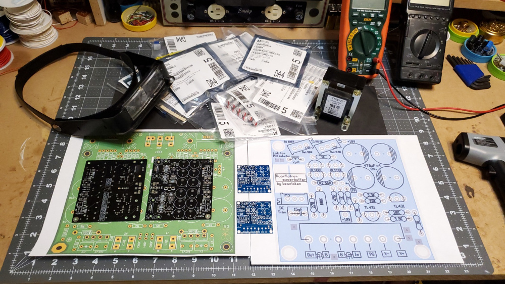
Earlier this week, I ordered the parts to build a pair of Kuartlotron superbuffers and VRDN power supplies (voltage regulator de-noiser). Got the PCB's from a4eaudio (thanks much). The buffer boards are tiny, only 2x2", so I scaled the board up to about 8x8" and printed it onto a full sheet of paper. Makes it much easier to read and stuff parts. I also have magnifiers, but I find it much more relaxing to work from a large printed copy. My plan is to use this buffer for testing tube type preamps on my bench.
If you are interested, here are some threads with detailed information and build instructions:


Comments
Bill, I have to be honest I thought you were stroking out when you typed the title to this thread. Looks like a cool product.
I'm still waking up and thought the black boards were what you were talking about at first. Then I saw the blue boards - those are small!
The bigger black boards are for the VRDN power supply regulator. I haven't started on those yet. I'm still working on and populating one of the two small blue buffer boards. Thought I'd have it running by now, but it has been a slow go so far. The on-line instructions are somewhat sketchy and the latest Bill of Materials (BOM) that I found was slightly out of date. Had to make a few Mouser part number substitutions for obsolete parts, but I think I'm good to go. Also, I found what appears to be the final schematic that matches the blue boards. I found a couple minor errors on the schematic so far, but nothing major. Hope to give it the smoke test sometime tomorrow.
Blue board schematic link:
http://www.fidelityforce.com/keantoken/content/Kuartlotron.php
Progress report:
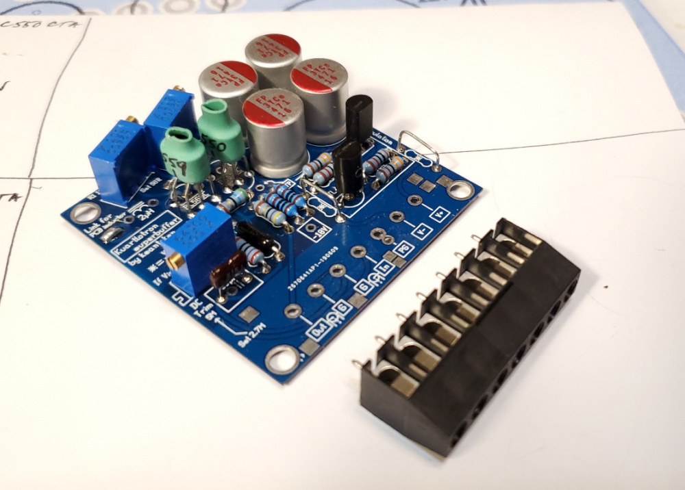
I have everything stuffed & soldered on one of the two small blue boards except the two transistor pairs and the long, black 7 position terminal block. I left this terminal block off for clarity, so I could take detail pictures showing all parts mounted so far. If you look closely, you will notice that I installed jumpers instead of resistors across the two resistors that are marked with an asterisk star type symbol (*). These two resistors are dropping resistors that are used to lower the incoming power supply voltage to the appropriate level needed at the input. Since I will be doing my initial power up with my regulated DC bench supply, I will only be applying the needed +10, 0, -10vdc to run the circuit. I therefore installed temporary jumpers instead of resistors. Later on, when I power the PCB up using a higher +/- dc voltage supply, I will remove the jumpers and install the appropriate size and value of resistor needed.
Note that I substituted a BC559CTA transistor for the BOM specified BC560CTA transistor. The BC560CTA is obsolete and no longer available from either Mouser or Digi-key. The BC559CTA is the same as the BC560CTA, except that it has a lower maximum collector to emitter or base voltage of only 30V. The BC560CTA has a maximum collector to emitter or base voltage of 45V. Since the circuit is only running at +/- 10vdc, I should be OK. Time will tell.
Also, as you can see in the photos, I matched the transistors into pairs using my Radio Shack DMM. Tomorrow I will be grouping these transistors into matched pairs and binding them together, back to back, using heat shrink tubing. I'll put a small dab of heat sink compound of the back of each transistor to improve thermal transfer. I know this sounds confusing, but once this is done I can solder the 6 terminals of each matched pair onto the PCB. I'll post some detailed pictures tomorrow showing specifically what this looks like.
Cheap and comes in handy. Wish I'd used this before soldering in some 'original nla parts' ordered from ebay. Would have saved a lot of money, time, and aggravation. https://www.ebay.com/itm/176044569303?itmmeta=01J50NZ75D31NRKT3ZSTDMF1KA&hash=item28fd12f2d7:g:JXoAAOSwREtlWySM&itmprp=enc:AQAJAAABAJoDhzrXoHSi9qjTqry8zBM2FmAziVnY2hezT0uhSzFIKq9+u2r3KxVpvTQDpLUskGEMSg2td59erXEB9t6eXQqYirNlxrKgQgj2EVHjwyrMD9XJXVJ3yvaCjKStXJWroUGMg7P8jeTimopK/1V5D9OzAoP+M7up3Y5/ZQHbCDDU+Yy1MoY+S08eXdrtnn0Q7oRwTc0Tc7snUxa0im31ZqS5Bb3zN0mS0e8RwrEQDFpuPcF/aq0OTUjSxMe9uBGt/k3n7LvIIHF/PYW5TUZsRgaQtJYyCbq4kYx2f019JkSGqMr78hCXdsEEJZxY1thLMFADiVIkk5o54+hFdgw5tow=|tkp:Bk9SR-ry_JWoZA
Looking good! I'll be curious how this works out for you and how low the ripple is compared to just a simple 3 legged regulator with a big cap behind it.
Agreed. I'll have to get one of those for doing quick checks. I used my Radio Shack DMM to test and match transistor gain because I was too lazy to set up my B&K transistor curve tracer for this project. The curve tracer can do a much better job of testing the transistors at the actual operating voltages and currents, but it is not as handy.
Thanks, Tom. I hope to make this comparison as well. I have a simple 3 legged regulator board all set up and ready to test.
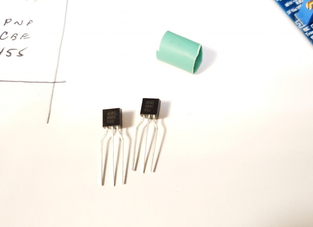
More progress today. I assembled two pair of thermal tracking transistor bundles. This is done for stability, so the buffer's DC offset does not drift up and down with temperature.
One gain matched set of BC550CTA transistors:
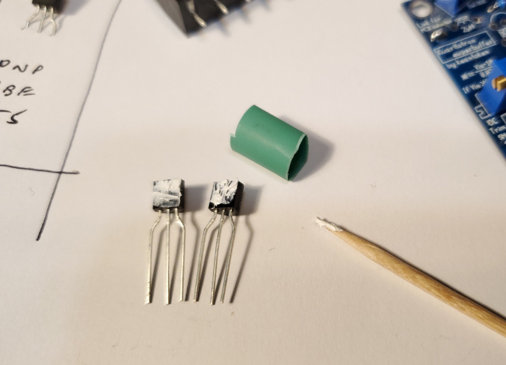
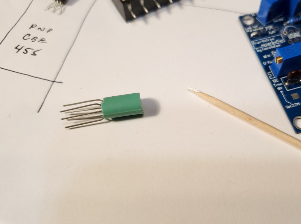
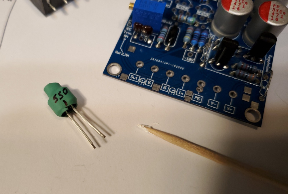
I applied a thin layer of heat sink grease to the transistor faces with a toothpick:
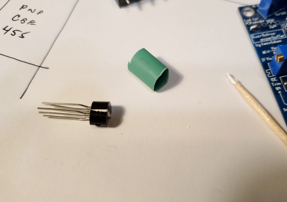
Then I squished the two faces together to form a 6 legged bundle:
Then I slid a short piece of heat shrink tubing over the transistors:
And secured the heat shrink in place with a heat gun:
And soldered them onto the PCB:
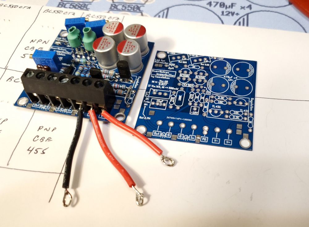
Then I installed the 7 position terminal block and some power supply hook up wires. The PCB is now ready for the smoke test!
Very cool.
Whoo-hoo! Success! Brought it up slowly with my DC bench supply to approx +/- 9.8vdc. Circuit draws about 10ma or so from the supply. No smoke. No loud pops or buzzing noises. No explosions. Oscilloscope shows a ruler flat frequency response from 20 to 20kHz. 1Vrms input at 1kHz produces 0.736Vrms at the output. Using a +/-9.8vdc power supply, clipping occurs with about 5Vrms applied to the input. A 1kHz sine wave and 10kHz square wave look very clean (see below).
I adjusted the 3 trimmer pots for the lowest possible input and output DC offset voltage, which turns out to be about 4mv dc. I can trim the DC offset down to less than 1mv on either the input or output circuits individually. But I cannot do it simultaneously. When I adjust the output DC offset down to less than 1mv dc, the input DC offset goes up to about 8mv dc. Then, if I adjust the input DC offset down to less than 1mv dc, the output DC offset goes up to about 8mv dc. No big deal. A dc offset of only 4mv is still a very good measurement! So now I can start populating the VRDN power supply board to see if I can get that one working too.
Before moving on to the VRDN boards, I have one important PCB stuffing tip relating to the small blue buffer boards. I'm posting this as a "heads up" to anyone that might actually be interested in building this project. This board uses 3 small Bourns trimming resistors to adjust the DC offset and split the +/- voltage rails between upper and lower transistors. On the schematic, they are listed as R1 (a 100 ohm trimmer), R5 (a 5k ohm trimmer), and R9 (a 5meg ohm trimmer). The instructions tell you to pre-adjust these trimmers to specific values BEFORE you solder them onto the PCB. The specific values are printed on the PCB boards as follows: R1 should be set to 56 ohms, R5 should be set to 3.6k ohms, and R9 should be set to 2.7meg ohms. The reason that you want to adjust these BEFORE soldering is because these trimmers are in parallel with other parts on the board. They therefore cannot be adjusted properly AFTER you solder them in place.
In addition to the above problem, it is also very difficult to put test clips on the small pins and adjust the trimmer value before soldering them onto the board. So you might be tempted to solder them in place first and then adjust the values later. Don't do this. Adjust first, then mount and solder. In order to make it easier to make these adjustments, I mounted each trimmer onto my Radio Shack breadboard, placed a jumper across pins 3 and 2, and then measured the value with my mini-grabber clips connected across pins 3+2 and pin 1. Pin 3 is the pin closest to the adjustment screw and pin 2 is the center pin. (see mfg datasheet for the pinout listing on these units). Pin 1 is the pin that is furthest from the adjustment screw. Pins 3 and 2 are shorted together on the PCB such that the trimmer becomes a simple adjustable resistor value when soldered in place. My description here is probably about as clear as mud, but you have to get this set up correctly, otherwise you will get very large DC offsets when you do the initial power up.
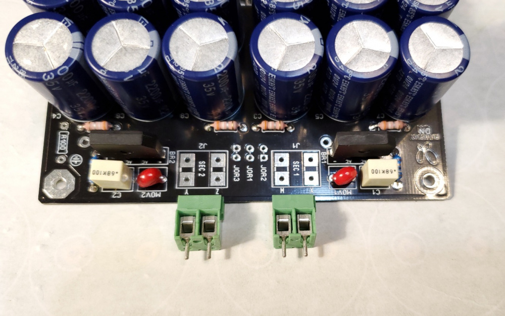
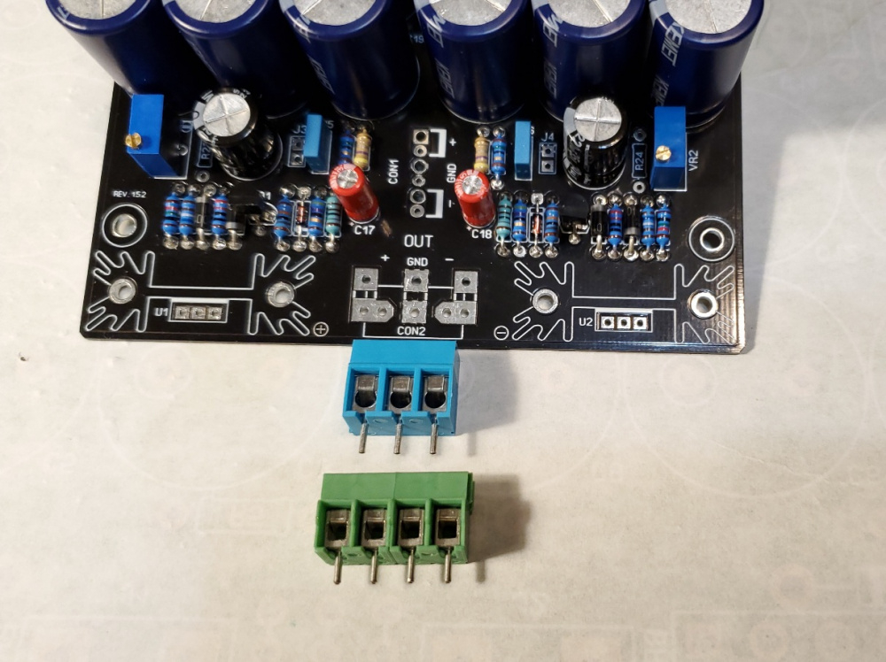
Update: Still working on stuffing the VRDN power supply PCB. Ran into a few snags. This was due to the fact that the Bill of Materials (BOM) that I used for ordering parts was the old BOM from the original PCB. The PCB that I am using is actually a later revision that was produced by someone who was reading the long 42 page DIYaudio thread and then decided to make his own PCB's on page 39. Most of the parts are the same as the original board but there are a few important differences (also see pics below).
1) Different LM317/LM337 regulator heatsinks
2) Different transformer input terminal blocks
3) Different power output terminal blocks.
I'm not complaining. I'm just mentioning this because if someone were to try to build this circuit from scratch, these will be the kind of "snags" that you will run into. Just one of the "joys" of DIY circuit building from a very long 42 page DIYaudio thread!
Heatsink comparison below. The correct, replacement headsink is shown on the left side. The original heatsink is shown on the right side. Note how the mounting pins do not line up on the right side. But the left side replacement heatsink is a perfect match to all the pins and silk screen printing. Luckily, I found these replacement heatsinks locally at the American Science and Surplus store. If anyone is interested, I put together a complete, revised BOM that shows all the Mouser part numbers for this revision.
Terminal block comparisons below. The green terminal blocks are the originals that do not fit the revised PCB. The green 2 terminal blocks only have a pin spacing (or pitch) of 5mm, but the board requires a 2 terminal block with a 7.62 pin spacing.
Here the green 4 terminal block was the block from the original BOM, but it does not fit the revised PCB. Luckily, I found a 3 terminal blue terminal block in my junk box that fits perfectly. A replacement 3 terminal block can have either a 5mm or 7.62mm pin spacing (or pitch), but it can only have 3 terminals, not 4.
I powered up the VRDN power supply today. No smoke or fireworks. To be safe, I used my dim bulb tester and variac. In the picture below, a Triad VPS24-3300 transformer with dual 12vac secondaries feeds into the dual secondary inputs of the VRDN PCB board. I connected two 680 ohm 2W resistors to the VRDN boards output terminal blocks to act as a dummy load. They got slightly warm to the touch during the test, dissipating about 1/3W each.
After carefully adjusting the two blue multi-turn trimmer pots, the output of the VRDN board locked in to a tightly regulated +/- 12vdc. AC ripple (or noise) measured roughly 1 to 2 mV rms using my two DMM's (see pics).
This small amount of ripple is probably just noise being picked up by my long DMM meter probes and other wiring. So, to eliminate this unwanted noise, I fired up my oscilloscope and attached the special low noise ground clip to the end of the probe tip (see pic). Even at full scope sensitivity, I could not measure the ripple or noise level. It was simply below my ability to measure. Will this make a difference in the sound or my ability to test tube preamplifiers? Probably not. But it is good to know that the "de-noising" circuitry in the power supply appears to be working properly.
I now have the Kuartlotron superbuffer and VRDN power supply fully debugged and working well together. Per the DIYaudio thread instructions, I am using a pair of 68 ohm resistors in the buffer board's two spots marked with an asterisk (*). These resistors, together with 6 other parts on the board, help to drop the VRDN power supply voltage of +/- 12vdc down to a tightly regulated +/-10vdc that is needed by the superbuffer circuit.
Everything seems to be working just fine at this point. I was able to tweak the R9 trimmer pot to get the DC offset down to about 2.4mv on both the input and output connections. Frequency response is ruler flat from 20-20kHz. Sine and square waves are very clean. Noise is below my ability to measure. I have not done an REW harmonic distortion profile test yet, but that is on my agenda.
Since the long DIYaudio thread instructions are somewhat difficult to interpret, I am putting together a listing of my personal step by step procedures that I used to build and properly adjust both of these boards. I'm doing this while the entire process is fresh in my memory, in case I ever want to build another one these boards down the road. (ie., six months from now, I won't be able to remember all the details). If you are interested, send me a PM and I'll forward you a copy of my personal step-by-step instructions.
The designers of the VRDN power supply made it possible to power the supply using a simple AC to AC type wall wart instead of using a standard transformer with dual secondaries. Instructions in the DIYaudio thread show how to do this by simply swapping out a hand full of parts on the PCB.
Since I already had an unused Jameco 1000ma 16V AC to AC wall wart in my junk box, I decided to give the wall wart idea a try. This actually worked out quite well. Ripple & noise is just as low using the wall wart and the music from my phone sounds just as good. The buffer circuit, when placed between my phone and the Lepai 2020 amp, has more than enough output to play my bench speakers as loud as I want.