Site Links
Howdy, Stranger!
It looks like you're new here. If you want to get involved, click one of these buttons!
Quick Links
Categories
In this Discussion
Who's Online (0)
Cheap 8.5Wx2 (not 100Wx2) OCL Power Amp Build

100Wx2
I started building one of the cheap OCL power amp kits that are currently being sold on ebay and amazon. This is the one that xraytonyb used for his recent 10 part DIY training video: Link: 
OCL stands for "output capacitor-less." The circuit is almost completely DC coupled except for one protective 10uf coupling capacitor at the input. These kits are being advertised as 80 or sometimes 100Wx2, but they are really more like 15 or maybe 20Wx2, at best. They go for about 10 to 15 bucks each.
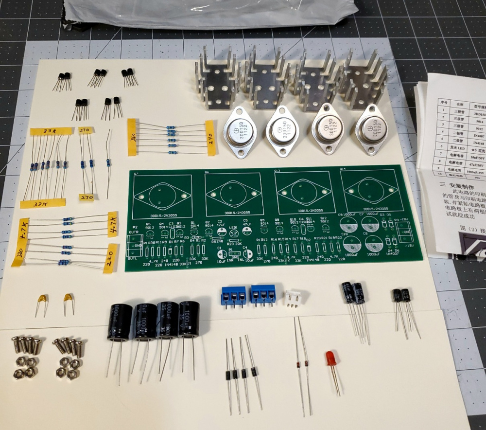
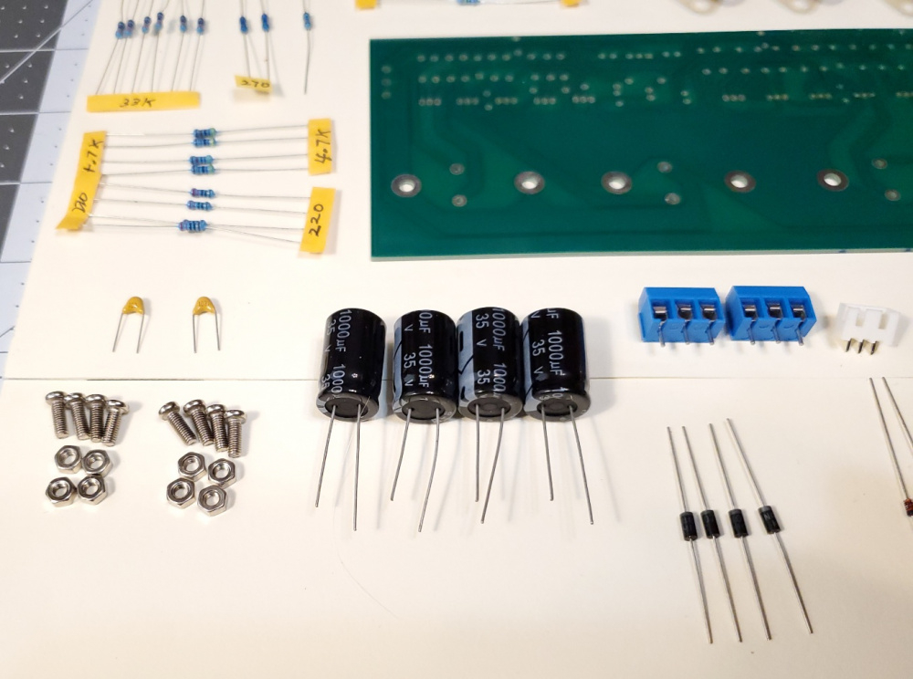
If you want to give this circuit a try, note that two different versions appear to be available on ebay and amazon. The two versions have slightly different PCB layouts and schematics, but the transistors used are the same. The dark green PCB version does not have holes for mounting it in a cabinet with standoffs. The light green PCB version, however, has 4 holes on the ends for standoffs. Since they were cheap, I ordered both versions. With each kit, you get a small bag of discrete semiconductors, caps, resistors, heat sinks and a PCB (see pic). No power transformer or case.
My goal will be to assemble the board, test it on my bench power supply, and then complete the project with a suitable case and power transformer. I'll stop back periodically with updates as I go along. Should be a fun project.


Comments
Looks like plenty of space to drill your own mount holes though at least.
Wonder what it would take to bridge them for monoblocks.
Not sure if this amp's output configuration can be bridged. Perhaps someone else can answer that question. While it looks like there is plenty of space for mounting holes, you would actually be drilling through PCB traces at each corner. Three of the corners would involve drilling through traces held at ground potential while one of the corners would be at the negative voltage rail potential (approx -18vdc). You could probably get around this problem by using nylon standoffs and screws. My guess is that the original design of this PCB called for mounting the four TO-3 package output transistors to an aluminum angle bracket that was, in turn, bolted to an aluminum chassis or larger heat sink configuration. In this way, the board would be held securely in place without the need for standoffs. EDIT: Note that if you mounted all four output transistors to a common aluminum angle bracket, then you would have to install mica insulating washers and heat sink grease on each TO-3 style transistor when you mount them. If you did not, the case, which is the collector, of each transistor would short out. The output transistor's case cannot be allowed to touch another transistor case.
Bill, I love your projects!!
A quick excerpt pulled from wikipedia regarding bridging:
"Since two amplifiers are being used in opposite polarity, using the same power supply, the bridged output is floating. This makes a DC blocking capacitor between the amplifier and the load unnecessary"
Since these amp boards are using two power transistors per channel without output caps.... sounds awfully similar to the above description. So I bet these are already setup bridged for each output and probably can't be bridged again.
The output stage is a balanced configuration using two 3DD15 output transistors and a dual rail power supply of approx +18vdc, 0, -18vdc. The full schematic is shown in several of Tony's training videos. No output capacitor is used. DC balance with minimal offset (a few millivolts or so) is accomplished through a 33k resistor in the feedback network, connected to a matched pair of differential transistors at the input. Not sure if this can be bridged mono or not. Even if you could, I'm not sure I would want to. You would still only have about 30 to 40 watts or so. I'm thinking more in terms of experimenting with this amp as a lower powered computer desk or test bench amp. Maybe see how it will sound compared to the Lepai LP-2020a that I am currently using.
Thanks, David!
I was hoping to start on mine this weekend, but it looks like I'll be diagnosing a DOA monster Marantz receiver instead. Hopefully it's something simple and I then can start planning some kind of chassis for this amp kit.
eBay links?
Below are two links, John. I just went to ebay and amazon and typed in "OCL power amplifier kit" The ebay link currently shows 30 sellers (take your pick). The amazon link shows 6 sellers. I bought my two kits (dark green and light green versions) from amazon. Can't remember which seller I clicked on. I'm still waiting for my light green kit. It is probably on a slow boat from China.")
https://www.ebay.com/sch/i.html?_nkw=OCL+power+amplifier+kit&_pgn=1
https://www.amazon.com/s?k=OCL+power+amplifier+kit&crid=3AH0730ZNRUDH&sprefix=ocl+power+amplifie+kit,aps,1028&ref=nb_sb_noss
Also, I just noticed, there appears to be 3 versions of this kit, not two. 1) light green PCB version, 2) dark green PCB version without mounting holes, and 3) dark green PCB version WITH 4 mounting holes. The blue boards also listed in the above links are actually a different amplifier kit; not another variation. Tony mentions another version in the first video with a slightly wider PCB, but I have not seen that one.
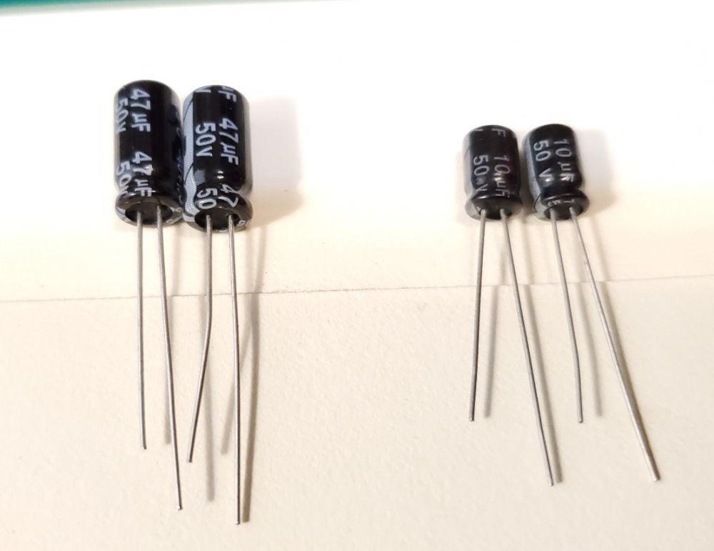
I populated the pcb with all resistors, diodes, and most caps. I replaced the two 10uF 50V input coupling caps with Elna 10uF 35V Silmic II types. Elna discontinued the silkies a couple years ago, but I still have a small stash of them. Next up will be installing the four big 1000uF caps and all transistors.
I picked up a used B&K 501a semiconductor curve tracer a couple years ago. So I tested all the supplied S9014 and S9012 transistors supplied with my kit. All the transistors matched fairly close right out of the bag, so this testing process was probably overkill on my part. I grouped the six S9014's in sets of two and will be using the best match from this group for the input differential pair. This should help to keep DC offset on the output as low as possible. The four S9012's did not match quite as well, but that should not create a problem. In the video, Tony did not match transistors at all and he didn't seem to have a problem with DC offset.
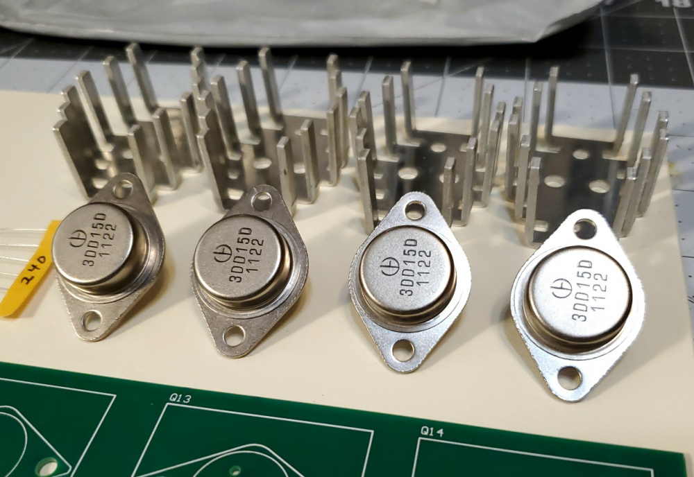
I also tested the four T0-3 output transistors. One pair was a fairly close match, but the other pair was not. But, per Tony in the video, the output transistors do not need to be matched.
Smoke test:
Only 5 volts, what could go wrong?
But the voltage on the pcb was coming up double what it should have been, so I quickly powered down. Re-checked my connections and discovered that I had the bench power supply DC wires connected to the wrong terminals. I was trying to make a 0, +5vdc, -5vdc type connection when I should have been making a +5vdc, 0, -5vdc connection. So I swapped out the wiring and this time it worked:
DC offset at the speaker terminals was -2.1volts, which is very high, but that is what it should be at very low supply voltages, because only 1 of the 2 power output transistors is conducting. So I brought the voltage up to +12vdc, 0, -12vdc and the DC offset dropped to 15.8mv. And total current drawn dropped to about 10ma. Excellent. And no smoke!
Encouraged by this result, I brought the voltage up to +18vdc, 0, -18vdc. This time the DC offset climbed up to about 45mv at the speaker terminals, which is borderline acceptable. So I will need to address this somehow. Total current flowing, however, remained at about 10ma.
So far, so good. These results are very close to what Tony got when he powered up his OCL amp in video training series part 3. Link: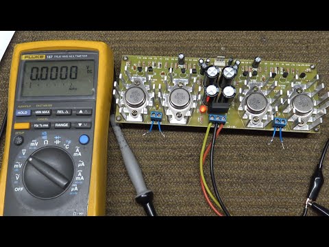
Next up will be playing some music to see how it sounds and then testing the power output at various voltage and current levels to determine what type of center tapped transformer I will need to buy.
Looking good, Bill! Glad you didn't see any smoke. Are you going to do the offset mod? I can't remember if I ordered the trimmers on my last Mouser order or not.
Thanks, Tom! I'm thinking about adding it. 45mv is quite a bit of offset. I closely matched the differential input pair before soldering them in place and was really hoping for a much lower offset, but it simply didn't happen. But I think I might have an idea as to where I went wrong. When I matched the transistors with my curve tracer, I had the voltage level set to about 10 volts DC. I could have set the testing voltage higher, but I thought that 10 volts was "good enough." When I powered up the OCL amp, I varied the voltage up and down from +5vdc,0,-5vdc to +18vdc,0,-18vdc. As I varied the voltage up and down, I noticed that when I got to right about +10,0,-10vdc the offset dropped to about 1mv!! At 12 volts, the offset crept back up to 15mv or so. So my input differential transistors might be perfectly matched for the temperature they reach when I apply 10vdc to them!! When I apply 18vdc, they might be heating up to the point where the match disappears. So, I'm going to pull these transistors and re-test them at 18 volts to see what happens.
If that does not pan out, I'll have to install Tony's offset circuit. It's only 6 parts and I could make up a small PCB like Tony did. If you did order the trimmers, could you send me the mouser part number that you used. I think that is a special 10 turn 5k trimmer with standard breadboard pcb pinout spacing.
In case anyone is interested, the subject of dc offset mods, was covered in part 8 of Tony's training video series linked below:
I did get the trimmers!
https://www.mouser.com/ProductDetail/Bourns/PV36W502C01B00?qs=BqPwLKJeIrffwfpi4cR/yg==
Thanks, Tom. I added a pair to my "next Mouser order" list.
Looks like I'm staring on the amp kit! The big Marantz 2325 I was going to work on for a friend turned out to have an open primary on the power transformer, so he'll probably trade it or part it out.
Houston - we have a problem. Actually just a misprint on the green board.
R11 & R22 are 240 ohms, but my board is marked as 220.
They sent me a 10k for R23 instead of a 20k. It's just the dropper for the LED, but hate bright LEDs, so I'll put a 20k in there.
Ya, Tom, I had the same errors on my dark green board. R11 & R22 are marked 220 on the board, but the schematic and parts list shows them as 240. I used the 240's in these spots. I also got a 10k for the LED dropping resistor, R23. So I used an 18.2k from my parts bin and the LED lights up fine.
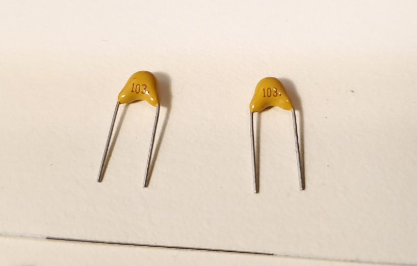
There is another error that I missed, but was discovered by Tony in the first two videos he did on the dark green pcb board 6 years ago. He found that the small ceramic cap, C3 and C6, should actually be 100pF, not 10,000pF. This is the small little cap marked "103" on its surface. When you measure it, it comes out as 10,000pF. He replaced both caps with a small ceramic 100pF from his parts stash. I still have the 10,000pF ones soldered onto my boards, so I need to pull them out and replace them. Here is a link to Tony's two videos from 6 years ago on the dark green PCB version of this amp (the board was actually a light brown color back then. Now it it is dark green, at least the ones sold by amazon):
I hooked my completed board up to my 8 ohm dummy load and then sent a 1kHz sine wave into the inputs. Applied +/- 18vdc from my bench supply. Hooked my scope to the outputs. I'm getting very high crossover notch distortion at very low output power levels (only 150mv at output). So I need to troubleshoot the problem before testing it at higher power levels.
Hmm...not enough bias voltage?
I just realized the schematic Tony is showing is slightly different from what I got with my kit. He has two 1n4148 diodes at the driver's bases. And look at R24 & R26 on his.
Tom, I know its confusing, but there are two slightly different versions that Tony built. In the 6 year old video, Tony built the version that we are building now, using the dark green boards. When he built this 6 years ago, the board was a light brown color, but it is identical to the dark green PCB that we have. Notice that this version has all the power supply components located off to the right side of the board. It does not use the 22 ohm resistors R24 and R26. There are also some other parts differences. But all the transistors in both versions are the same.
In the 10 part training video that Tony posted just this past year, he uses the light green PCB version. Notice that the power supply components are located in the center of this PCB. The numbering of all the parts on the two versions is different as well. I know it is confusing, but if you print a copy of the two schematics and lay them side by side you can see that they are "basically" the same. I will be building both versions. I'm still waiting for my light green PCB version, which is scheduled to arrive "Feb 9 to Feb 22" per amazon.
Yeah - I kind of figured that was the case. It's interesting that one version (caps in the middle) uses the two 22ohm resistors to decouple the differential and class A stages on the power rail, while mine does not.
-- I was just watching the older follow-up video you linked and he said he had to change R9 & R18 to get rid of the crossover distortion.
Ahh - I should have said R7 & R18. I think he ended up using 470 ohms.
I saw that too. That is probably why I am getting very high crossover notch distortion. My circuit has absolutely NO bias. I also need to change C3 and C6 from 10,000pF to 100pF. I found a handful of small 120pF ceramic disc caps and 1/4W 470 ohm resistors in my stash, so I am good to go.
I’m getting pretty close to firing this one up. I’m using Tony’s upgraded transistor substitutions - had to use a Ksa992 for the 2sa773 he used in one position. Pinout is different and had to do the leg twist, so we’ll see how that works out.
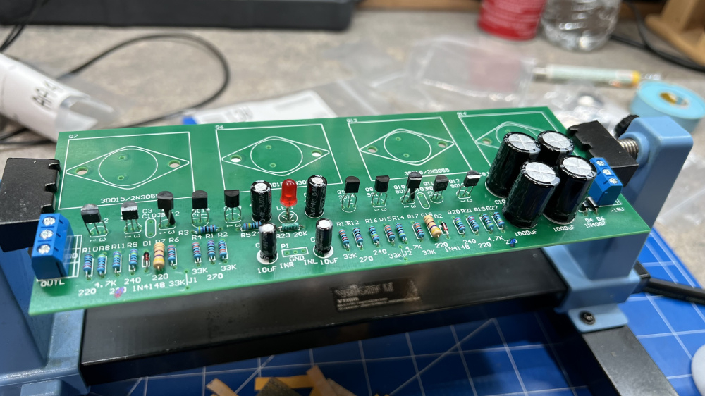
All that’s left are the TO-3s.
Here is what the crossover notch distortion looks like on my completely stock kit (no mods done yet). The two output transistors operate in "push-pull" to complete the upper and bottom half of the full sine wave. But because the transistors are not biased properly, one transistor shuts off before the other transistor begins to conduct. This results in a huge notch in the middle of the 1kHz sine wave.